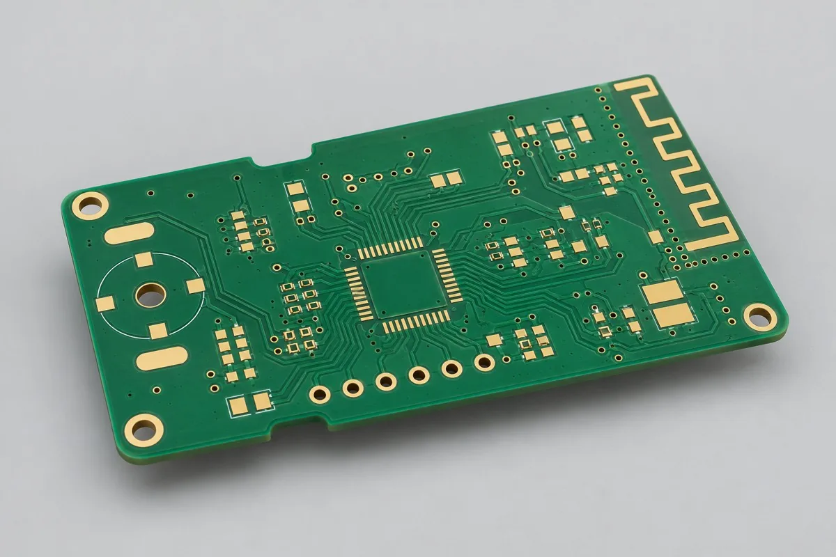
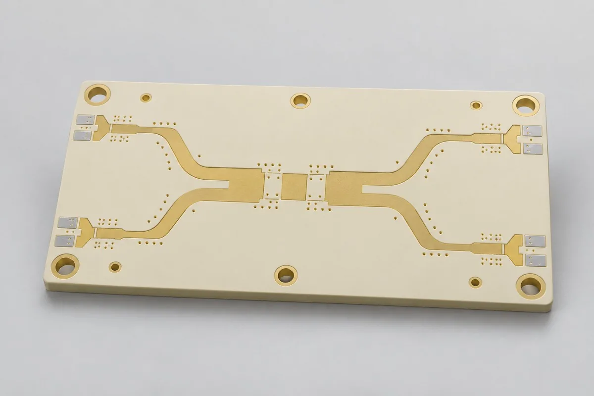
High-Frequency PCB
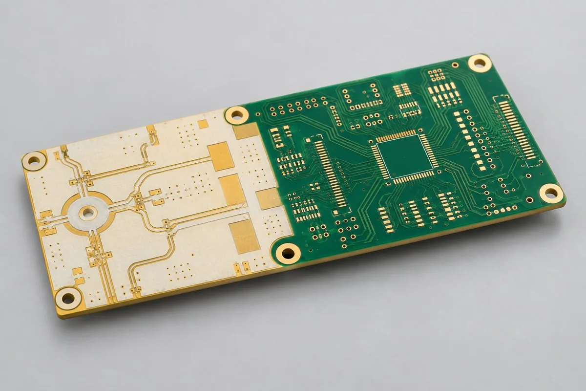
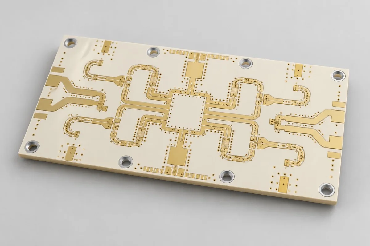
Compare high-frequency PCB materials, dielectric thickness, copper and finishes. Define RF geometry and measurement conditions for fabrication review.
View High-Frequency PCB ConfigurationsKFPCBA provides PCB manufacturing in Shenzhen alongside PCB assembly, component sourcing and PCB design support. Send the board files and requirements for a fabrication review, or start with the application and unresolved design questions.
A bare-board order covers the printed circuit board. Components, assembly, programming and product testing are separate work items that can be coordinated through our PCB assembly service.
| Project requirement | What to define | Explore the route |
|---|---|---|
| General control and interfaces | Outline, routing density, reference planes, finished thickness and connector geometry | Multilayer PCB · PCB prototypes |
| RF or controlled transmission | Exact laminate grade, stackup, critical nets, impedance and measurement conditions | High-frequency PCB · Controlled impedance |
| Power and thermal paths | Current paths, copper and via structure, dielectric thermal path and mounting interface | Heavy-copper PCB · Metal-core PCB |
| Dense packages or mechanical interconnects | Package breakout, every via span, bend state and rigid-to-flex transition | HDI PCB · Rigid-flex and semi-flex PCB |
These are selection routes. The manufacturing review must resolve the actual material, stackup and construction together; isolated reference values are not combined into a process limit.
BOM and component placement files are needed for assembly rather than a bare-board-only order. Use the Gerber, drill and outline checklist to check the package before the engineering RFQ. Incomplete inputs can be listed as open questions.
| Cost group | Comparison to make |
|---|---|
| Material and fabrication | Match material grade, stackup, copper, hole structures, finish and accepted delivery quantity. |
| Engineering and tooling | Separate one-time file preparation, dedicated tooling and special verification from recurring batch work. |
| Inspection and reports | Identify electrical testing, impedance measurement, microsections and any sampling or report requirements separately. |
| Delivery | Align panelization, depanelization, packing, shipping, taxes and trade terms before comparing totals. |
Use the PCB quotation comparison checklist to compare the same revision, accepted-board quantity, material, inspection and delivery scope. For repeat orders, identify reusable setup items and review material substitutions before confirming the new quantity.
Review material selection and stackup planning before choosing a reference configuration. Where a design still needs layout or constraint work, our PCB design service provides a separate starting point.
Agree the board identification, inspection scope and record package through quality planning. A fabrication electrical test, an impedance measurement and a microsection examine different things; one result does not replace the others.
For a first discussion, send the intended application, available files and quantity. We can then define the fabrication scope, questions to close and information required for a project quotation.
Quality and acceptance · Production equipment · Engineering RFQ with PCB files
Browse by product type, then compare configuration details, process tradeoffs, and verification requirements.
Compare high-frequency PCB materials, dielectric thickness, copper and finishes. Define RF geometry and measurement conditions for fabrication review.
View High-Frequency PCB ConfigurationsReview hybrid PCB stackups combining different material systems. Check lamination compatibility, thickness, via structures and impedance requirements.
View Hybrid-Material PCB ConfigurationsCompare Rogers PCB material grades and construction options. Specify the exact laminate, copper, dielectric thickness and RF acceptance requirements.
View Rogers PCB ConfigurationsSelect high-Tg PCB materials using thermal properties, assembly exposure and reliability requirements. Review the material grade with the intended stackup.
View High-Tg PCB ConfigurationsSpecify controlled-impedance PCBs with layer geometry, materials and target nets. Agree fabrication tolerances, test coupons and measurement conditions.
View Impedance-Controlled PCB ConfigurationsSelect FR-4 PCB construction by electrical, thermal and mechanical needs. Compare laminate grades, thickness, copper and fabrication requirements.
View FR-4 PCB ConfigurationsPrepare PCBs for lead-free assembly with suitable laminate, finish and thermal requirements. Verify material declarations for the actual order scope.
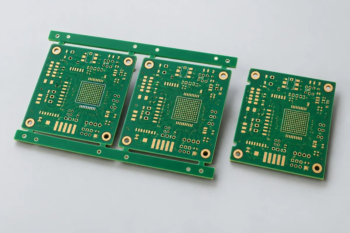
View Lead-Free PCB Selection ConfigurationsCompare HDI buildup routes, microvia layer pairs and fine-pitch breakout needs. Review stackup, via reliability and fabrication documentation together.
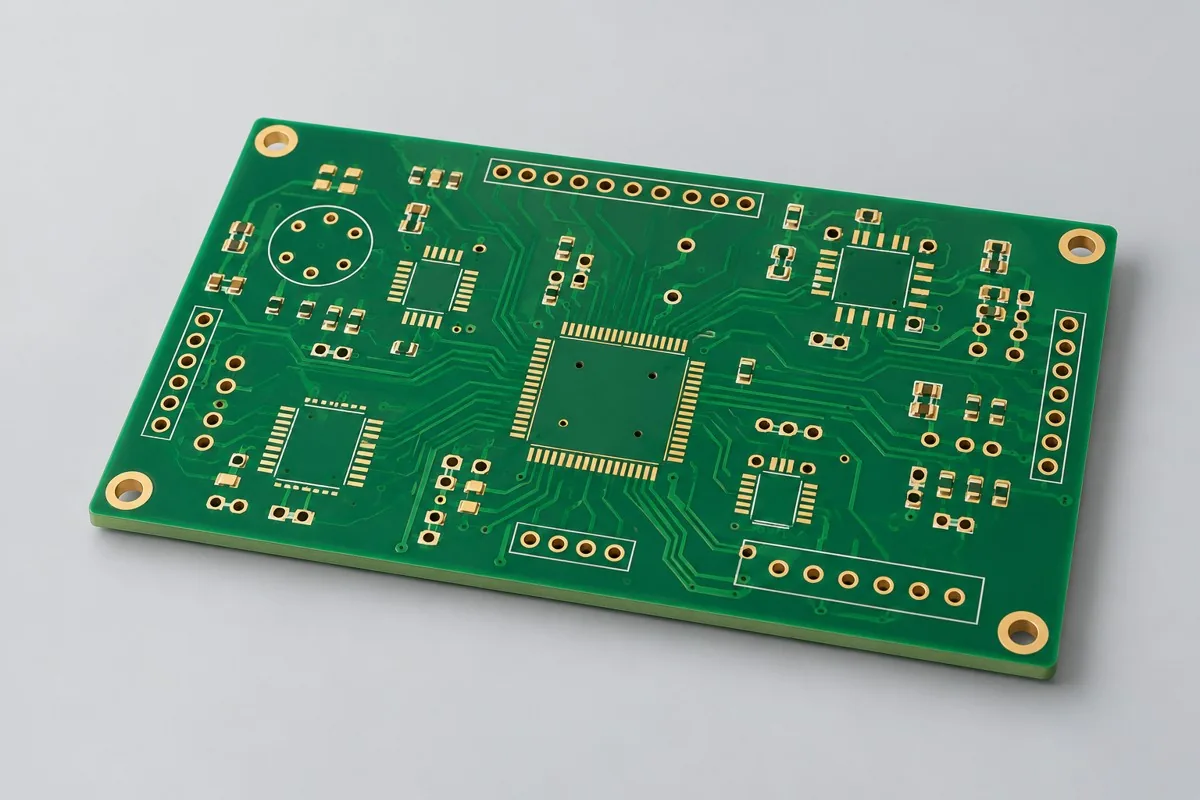
View HDI PCB ConfigurationsDefine multilayer PCB construction through layer order, planes, copper balance and via spans. Align stackup, impedance and electrical-test requirements.
View Multilayer PCB ConfigurationsReview RF PCB fabrication by signal path, grounding, connectors and measurement references. Specify material and geometry for the operating band.
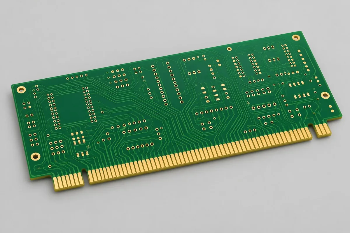
View RF PCB ConfigurationsSpecify PCB edge contacts by connector geometry, plating area, thickness and bevel. Separate mating-contact requirements from solderable surface finishes.
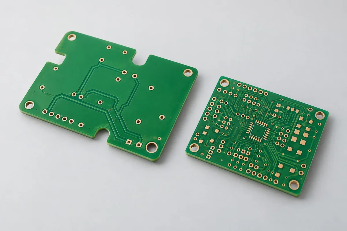
View Gold Finger PCB ConfigurationsCompare single- and double-sided PCBs by routing, plated holes and assembly needs. Prepare fabrication files, materials, finish and test requirements.
View Single- and Double-Sided PCB ConfigurationsCompare rigid-flex and semi-flex PCB constructions for static forming and interconnection. Define bend areas, materials, reinforcement and mechanical limits.
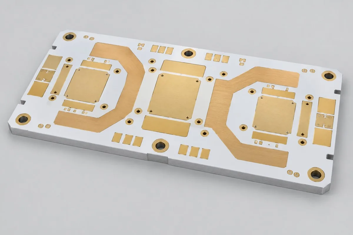
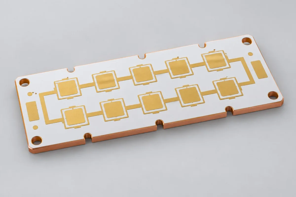
View Rigid-Flex and Semi-Flex PCB ConfigurationsCompare aluminum-core PCBs by dielectric insulation, thermal path and mounting needs. Review material, copper and fabrication requirements together.
Select metal-core PCB construction using thermal, electrical and mechanical constraints. Define insulation, copper, mounting and acceptance requirements.
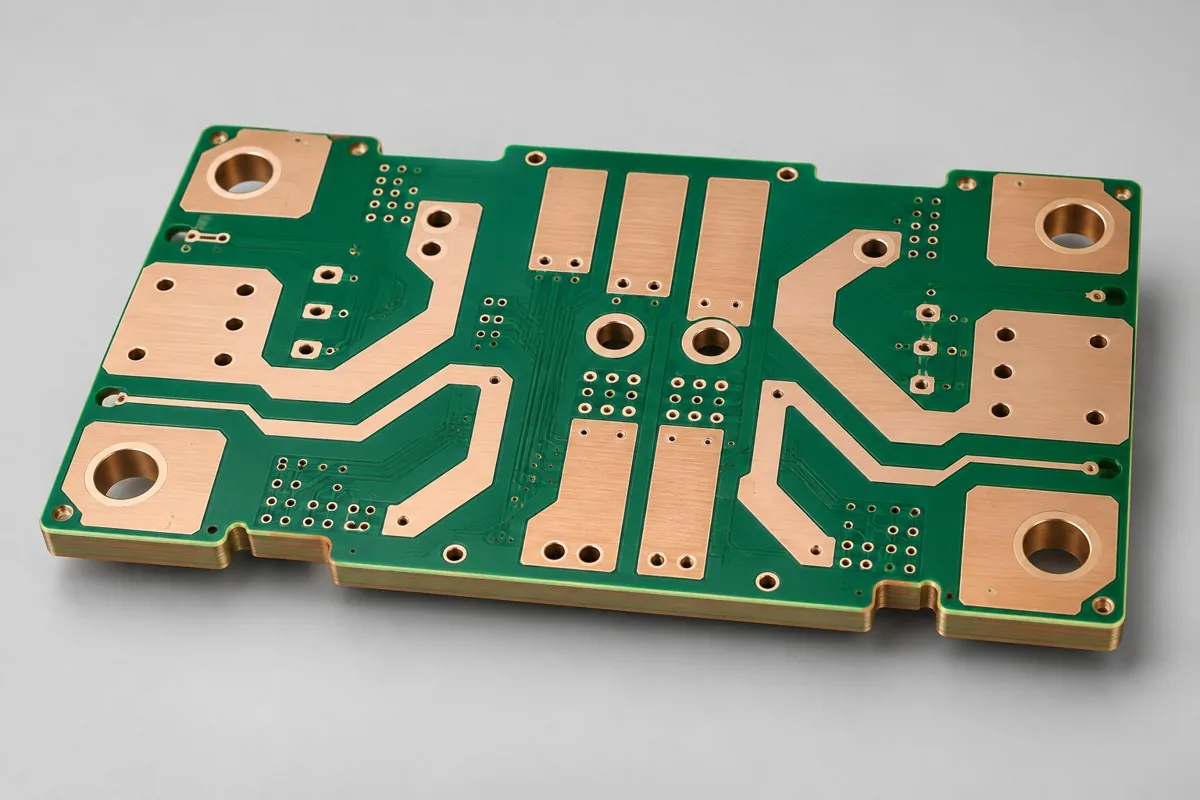
View Metal-Core PCB ConfigurationsReview heavy-copper PCB construction for current paths, heat spreading and fabrication constraints. Specify copper by layer and validate the complete design.
View Thick Copper PCB ConfigurationsPrepare a PCB prototype build with released files, material choices and validation priorities. Plan the changes needed before a repeat production order.
View PCB Prototyping Configurations
Tell us the product use and which files are available. We can define the next engineering step even when the data package is not complete.