
Company Address
201, Factory 6, Longhui Industrial Park, Fuqiao 3rd District, Xinhe Community, Fuhai Street, Baoan District, Shenzhen, Guangdong, China

Impedance-Controlled PCB

Specify controlled-impedance PCBs with layer geometry, materials and target nets. Agree fabrication tolerances, test coupons and measurement conditions.

Controlled-impedance PCB fabrication from defined nets and geometry

For a controlled-impedance PCB, send KFPCBA the relevant nets or geometry, target and tolerance, layer references and the intended inspection requirements. The label impedance-controlled is not a complete fabrication specification.

Material, dielectric thickness, copper, trace shape and reference geometry work together. Treat the stackup and critical structures as controlled inputs that must stay connected to fabrication and test evidence.

Specify the target and its verification relationship

ItemWhat to identifyWhy it matters
Transmission structureSingle-ended or differential mode, target, tolerance, layer and net/geometry identifiersA nominal impedance without a defined structure is ambiguous.
ConstructionApproved material, dielectric and copper definitions, reference planes and relevant fabrication allowancesA material or stack change may alter the critical geometry.
VerificationAgreed measurement method, coupon relationship, locations and reporting scopeA result must be connected to the boards and construction it represents.
ChangesApproval owner, proposed geometry/material change and affected recordsProduction clarification must not silently change design intent.

Connect fabrication checks with channel performance

An impedance coupon checks a specified manufactured structure. It does not by itself validate the complete connector, cable, device and routing path. Keep the board's electrical testing, agreed geometry measurements and system-level link checks as distinct evidence.

The controlled-impedance prototype checklist explains the review inputs. Where the stackup or routing is still open, start with stackup planning and impedance-controlled design.

Compare quotes with the same inspection scope

Align the actual construction, delivered quantities, coupon requirements, measurement records and any specified sections. Identify dedicated setup and recurring batch inspection separately. A lower total may reflect an omitted report or a different construction rather than an equivalent offer.

Material substitutions, via changes or an altered reference plane require assessment of the affected structures. Record approval and the replacement package before manufacture; do not reuse a result from another stackup as proof of the new one.

Send a traceable manufacturing request

  • Supply matching artwork, drills, outline and fabrication notes.
  • Identify critical nets, targets, tolerances and intended reference geometry.
  • Include the controlled stackup and material requirements.
  • State coupon, measurement and report expectations, including the acceptance basis.

Use the engineering RFQ for released files or a project inquiry to discuss unresolved inputs. The quality record plan should connect the agreed measurements to the released order.

Need a Configuration for Your Project?

Send the materials, quantity, target date, and available files for engineering review. Review quality and acceptance, material responsibility, or use the engineering RFQ when released files are ready.

Send Requirements

Product Configurations

Compare options by material, structure, and application. Each detail page explains the process and verification conditions.

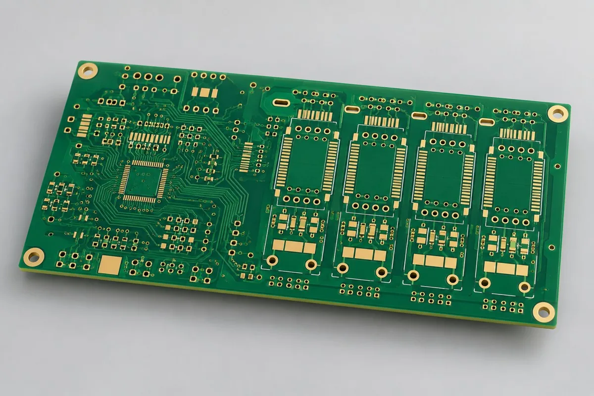
Illustrative configuration for Twelve-layer controlled-impedance PCB reference
Engineering Reference Configuration

Twelve-layer controlled-impedance PCB reference

Turn impedance objectives into net, geometry, stackup and measurement requirements. This illustrative twelve-layer configuration does not establish KFPCBA production history, automotive approval or measured impedance results.

Illustrative layer count
12 layers
Candidate laminate
S1000-2M; exact grade and supply documentation unverified
Reference objective
Controlled impedance; targets and tolerances remain undefined
Candidate finish
ENIG; layer requirements and acceptance need approval
View Configuration
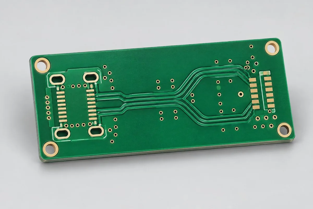
Illustrative configuration for DDR impedance PCB fabrication
Engineering Selection Reference

DDR impedance PCB fabrication

Review an eight-layer DDR acquisition PCB against controller, memory, topology, and fanout requirements. Define single-ended and differential targets by net and layer pair; bare-board TDR does not replace memory-link validation.

Material
370HR
Structure
8 Layer
Specification
1.60mm Target
Key Requirement
50Ω/100Ω target
Selection Focus
DDR Acquisition
View Configuration
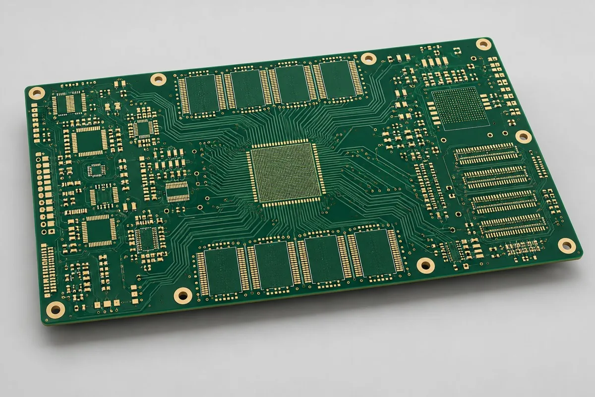
Illustrative configuration for Ethernet impedance PCB fabrication
Engineering Selection Reference

Ethernet impedance PCB fabrication

Ethernet controlled-impedance PCB fabrication reviews materials, structures, and deliverables against Ethernet nets and isolation boundaries, with cost breakdowns, one-time setup and same-revision reorder boundaries, selection steps, and quotation conversion methods. Specifications follow approved fabrication drawings; component assembly and complete-system verification are separate.

Material
370HR
Structure
6 Layer
Specification
1.60mm Target
Key Requirement
MDI100 Ω target
Selection Focus
ENIG
View Configuration
Illustrative configuration for USB impedance PCB prototyping
Engineering Selection Reference

USB impedance PCB prototyping

USB controlled-impedance PCB prototyping reviews materials, structures, and deliverables against USB differential definitions and connector regions, with cost breakdowns, one-time setup and same-revision reorder boundaries, selection steps, and quotation conversion methods. Specifications follow approved fabrication drawings; component assembly and complete-system verification are separate.

Material
370HR
Structure
4 Layer
Specification
1.00mm Target
Key Requirement
USB90 Ω Target
Selection Focus
ENIG
View Configuration
PCB / PCBA · PROJECT ENQUIRY

Does Your Project Need PCB Fabrication, Assembly, or Box Build?

Tell us the product use and which files are available. We can define the next engineering step even when the data package is not complete.

Call UsWhatsAppRequest a Quote