
Layer structure and package escape
Use routing density, reference planes, interfaces and package geometry to compare multilayer and HDI design routes.
KFPCBA provides PCB design and layout support alongside PCB fabrication and assembly. Start with the circuit requirements or an existing schematic, then define the design work, review milestones and source-file handoff for your project.
Our R&D and manufacturing coordination helps bring electrical, mechanical and production requirements into the same discussion. Firmware, specialized simulations, fixtures and product certification are separate work items whose ownership must be agreed.
| Starting point | What to bring | Scope to define |
|---|---|---|
| Product requirements | Intended function, power, interfaces, operating conditions and mechanical limits | Schematic responsibility, component selection, design stages and prototype objectives. |
| Approved schematic | Editable schematics, BOM, libraries, board outline and critical-net requirements | Placement, routing, constraints, reviews and manufacturing file generation. |
| Existing board or prototype issue | Design revision, source files where available, reproducible conditions and observations | Review, local modification or redevelopment, followed by a defined regression check. |
Gerber files are manufacturing outputs, not a replacement for a complete editable design project. If source information is missing, list the gap before agreeing the work.
| Stage | Outputs to agree | Release decision |
|---|---|---|
| Requirements and architecture | Requirement list, interfaces, power and mechanical boundaries, open risks | Do both parties mean the same product and operating conditions? |
| Schematic and parts | Schematic, BOM, component ordering codes and unresolved selections | Are function and component responsibilities clear enough for layout? |
| Placement and routing | Board source, stackup, critical constraints, library references and review findings | Do electrical, mechanical, assembly and test-access requirements fit together? |
| Manufacturing handoff | Gerber or agreed fabrication outputs, drills, BOM, placement data, drawings and revision list | Do exported files correspond to the same approved source revision? |
| Prototype verification | Agreed test cases, observed results, issues and controlled changes | Which requirements have been checked and which still need work? |
Use the PCB design brief and deliverables checklist alongside our design capability scope and DFMA review. Agree source-file rights, tool versions and library obligations before fixing the scope for layout-only work, development from requirements or an existing-board revision.
Use routing density, reference planes, interfaces and package geometry to compare multilayer and HDI design routes.
Define topology, stackup, return paths and model responsibilities for high-speed design and RF layout.
Set electrical boundaries, heat paths, connector geometry and installation conditions before choosing a thermal design route or rigid-flex structure.
Reference designs explain choices and verification methods. Their example numbers are design inputs rather than KFPCBA production limits or evidence of a delivered customer product.
Separate requirements work, schematic development, layout and agreed verification from prototype PCB fabrication, purchased components and assembly. Also identify software, fixtures, specialist testing and change requests that are outside the quoted work.
The development cost and scope guide provides a comparison method. A low total is not comparable if it excludes source files, circuit responsibility or the tests needed to accept the design.
Initial contact can begin with the intended function, existing files and target delivery stage. The team can then identify inputs to resolve and the design package to quote.
ELECTRONICS DESIGN · FROM REQUIREMENTS TO PROTOTYPE
Start with circuit, interface, and mechanical requirements, then compare the design inputs, stage deliverables, tradeoffs, and prototype-verification approach.
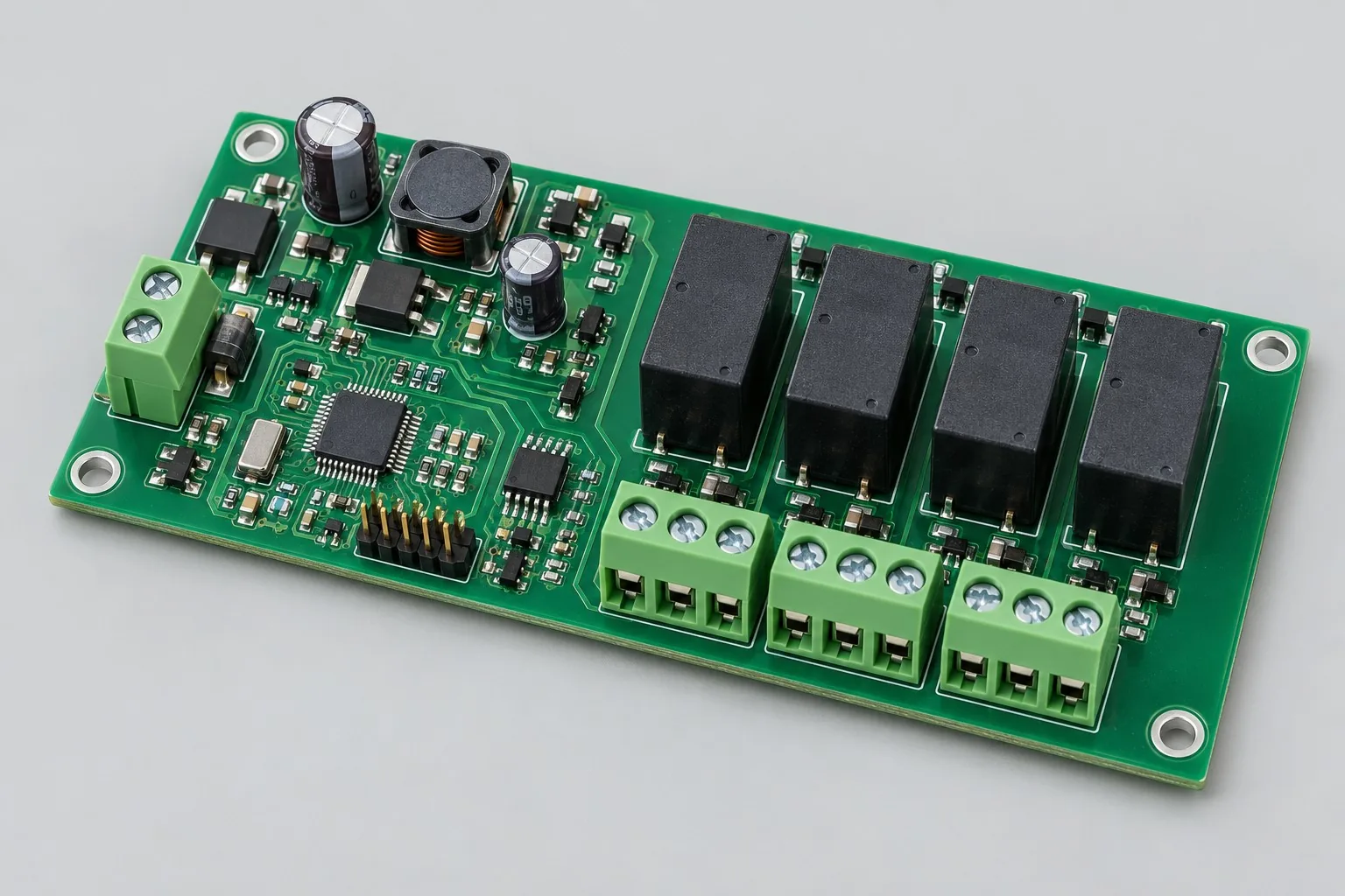
Plan single- and double-sided PCB layouts around power, routing and connector placement. Define relay loads, fault states and the manufacturing handoff.
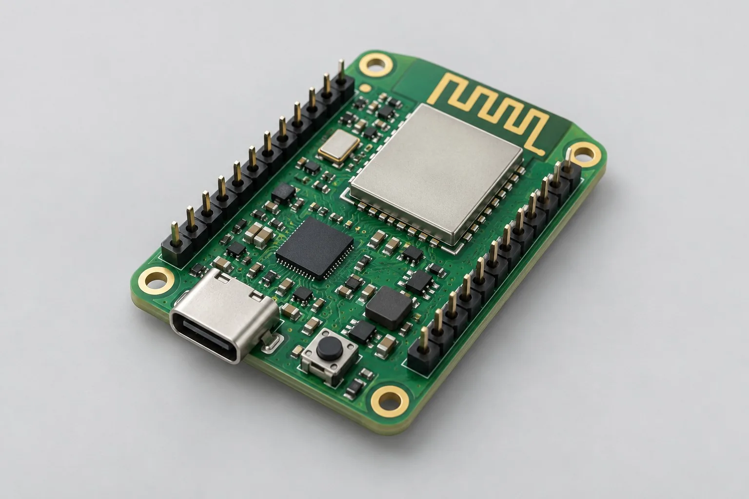
Choose an HDI design approach using package breakout, board outline and routing density. Coordinate microvias, antennas, batteries and fabrication constraints.
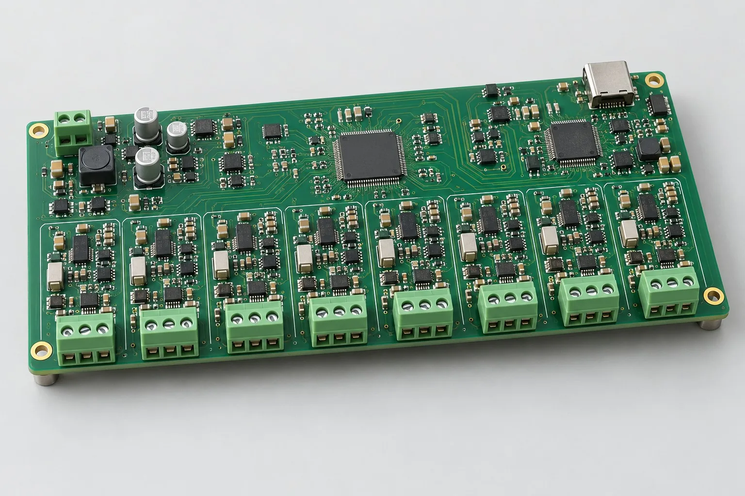
Plan multilayer PCB design for acquisition, industrial Ethernet and current-loop circuits. Define reference planes, isolation, clocks and calibration needs.
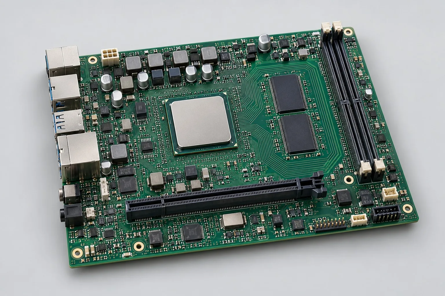
Plan high-speed PCB design around interfaces, topology, reference planes and models. Define DDR constraints and validation tasks before layout.
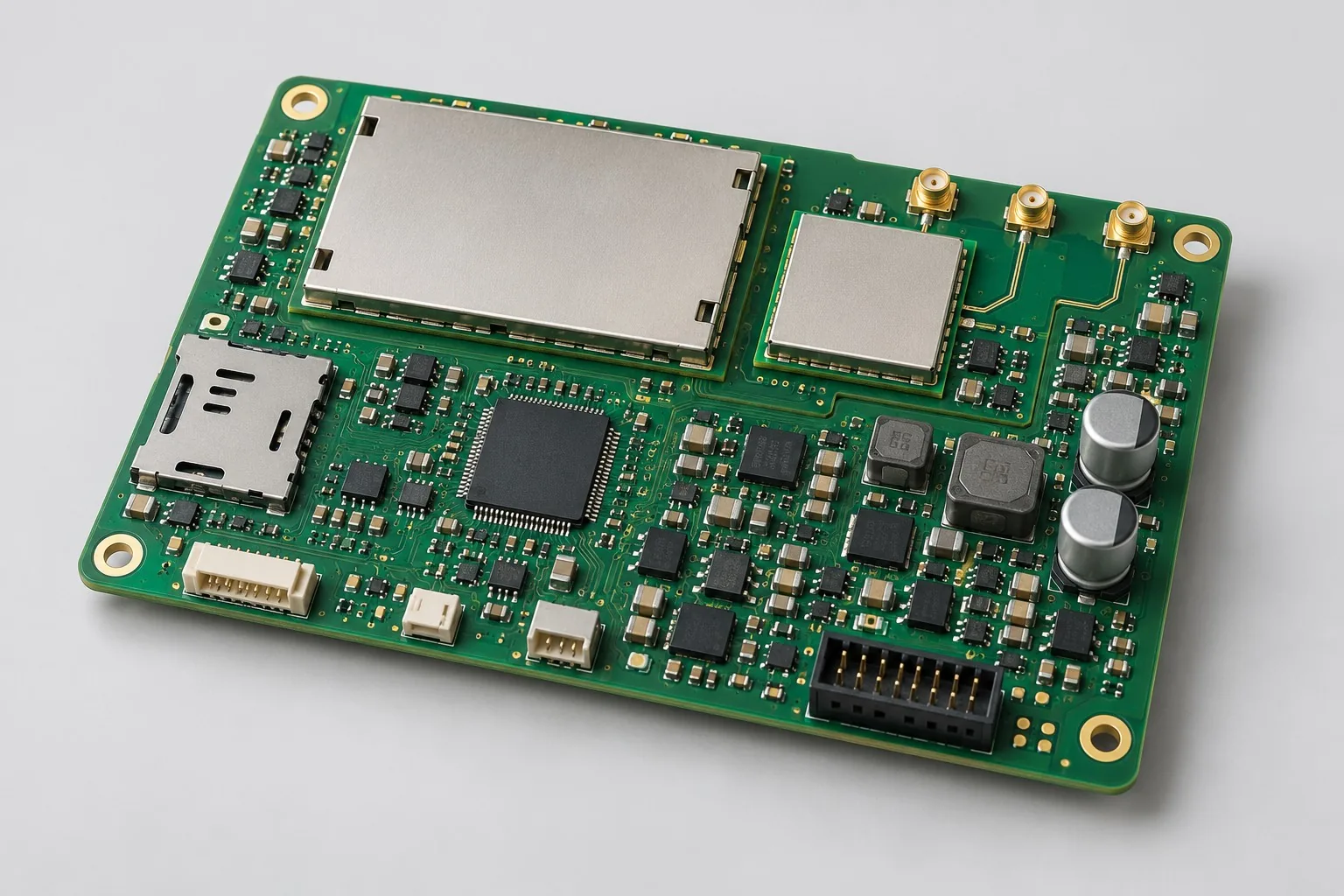
Review RF layout for positioning and wireless boards. Coordinate antennas, power, grounding, coexistence and test connections within the mechanical envelope.
View Design Requirements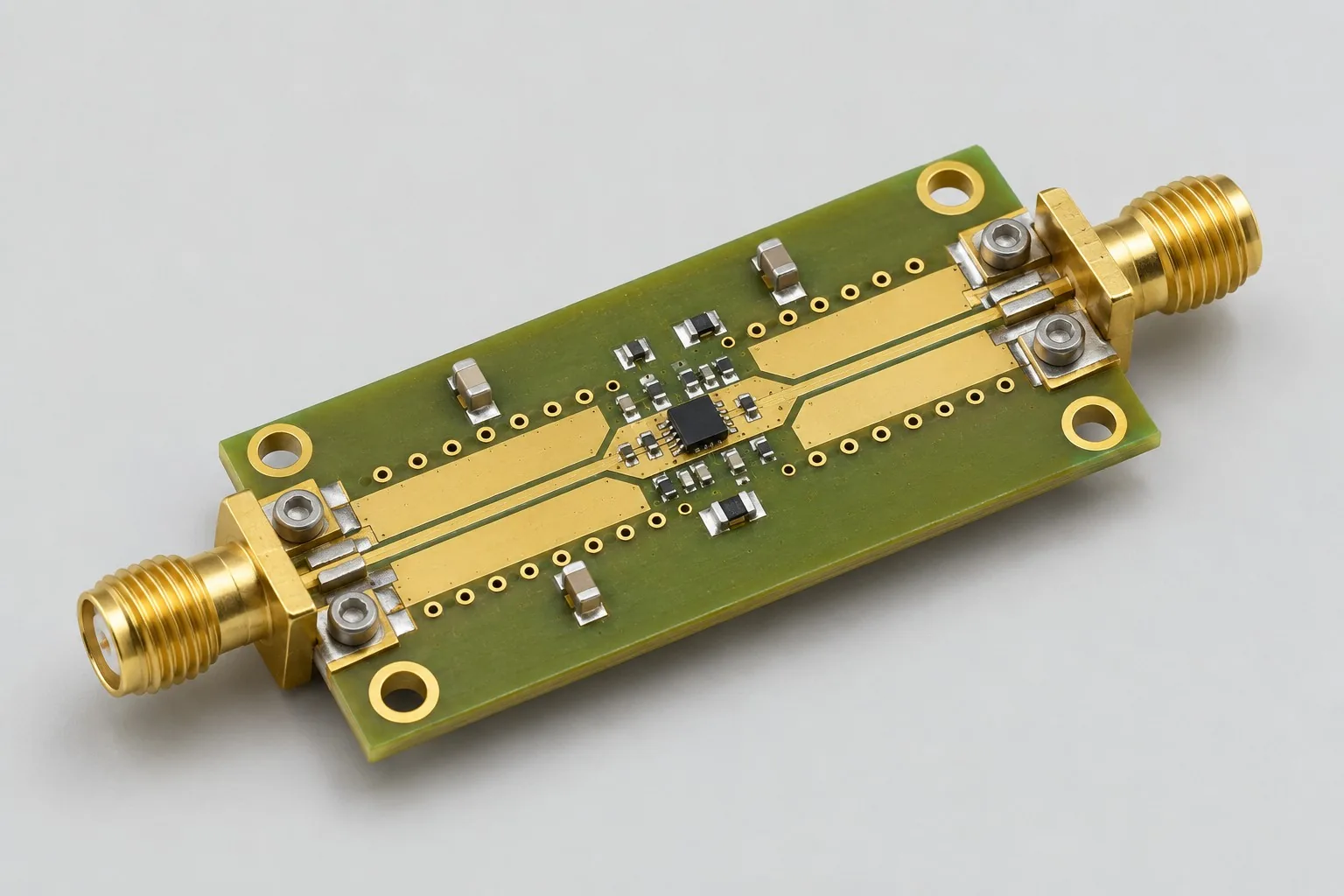
Define high-frequency layout requirements for through paths, filters and power dividers. Set reference planes, amplitude, phase and isolation targets.
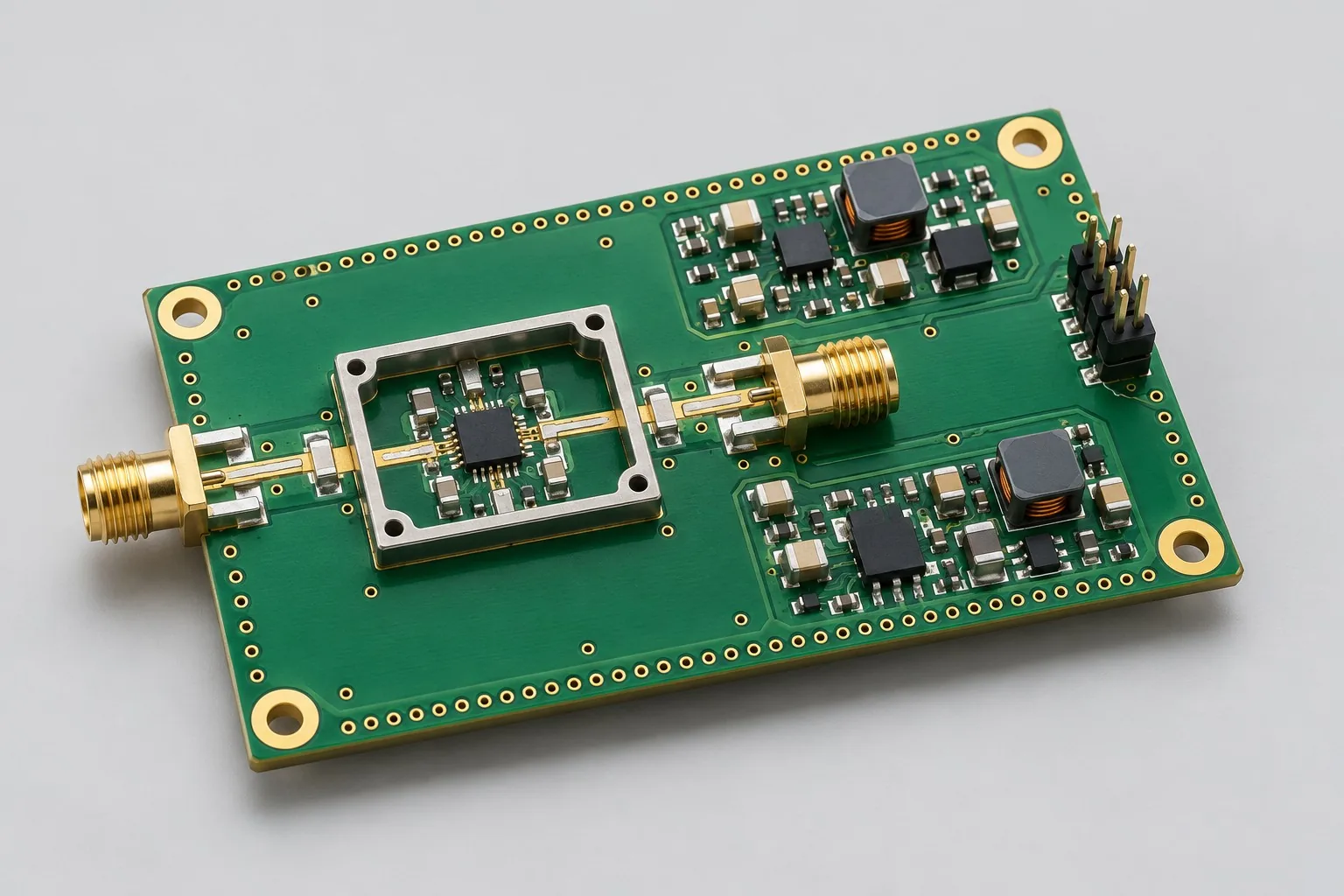
Plan amplifier PCB design around operating band, gain, bias, matching and thermal conditions. Define stability and compression tests for the prototype.
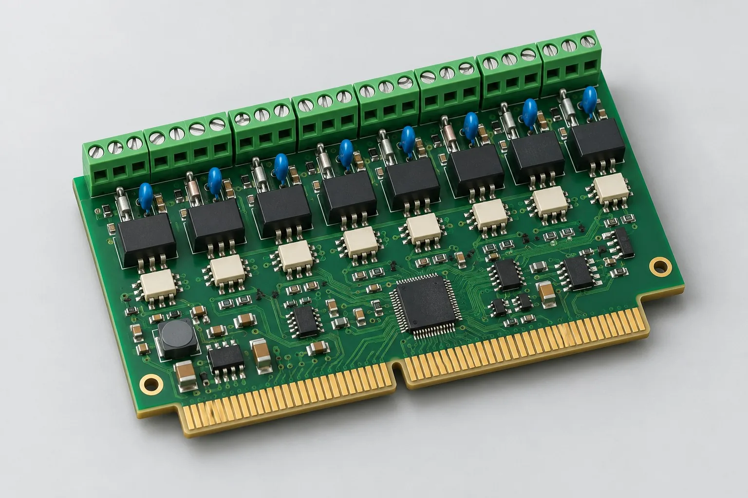
Plan gold-finger PCB layouts using the baseboard pinout, contact geometry and current requirements. Coordinate mechanics, signal conditioning and validation.
View Design Requirements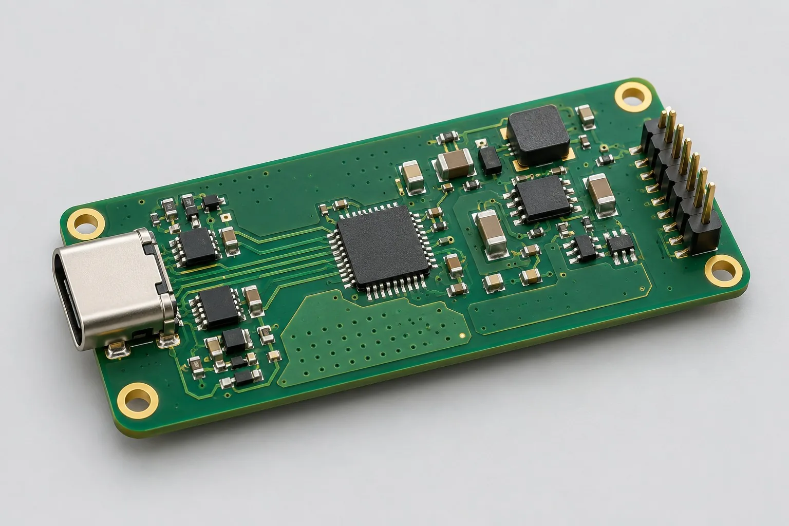
Define impedance-controlled PCB layouts using interface requirements, stackup and geometry. Coordinate routing constraints with fabrication and validation.
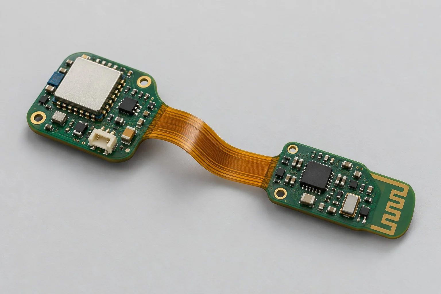
Plan rigid-flex PCB design around bend location, forming cycles, interconnects and reinforcement. Distinguish static installation from repeated flexing.
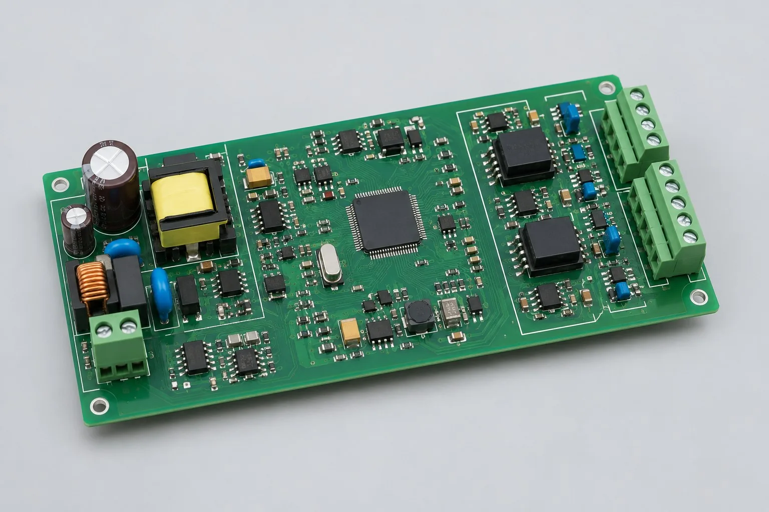
Specify halogen-free PCB materials through the exact grade, declaration scope and stackup. Review electrical and thermal requirements alongside compliance.
View Design Requirements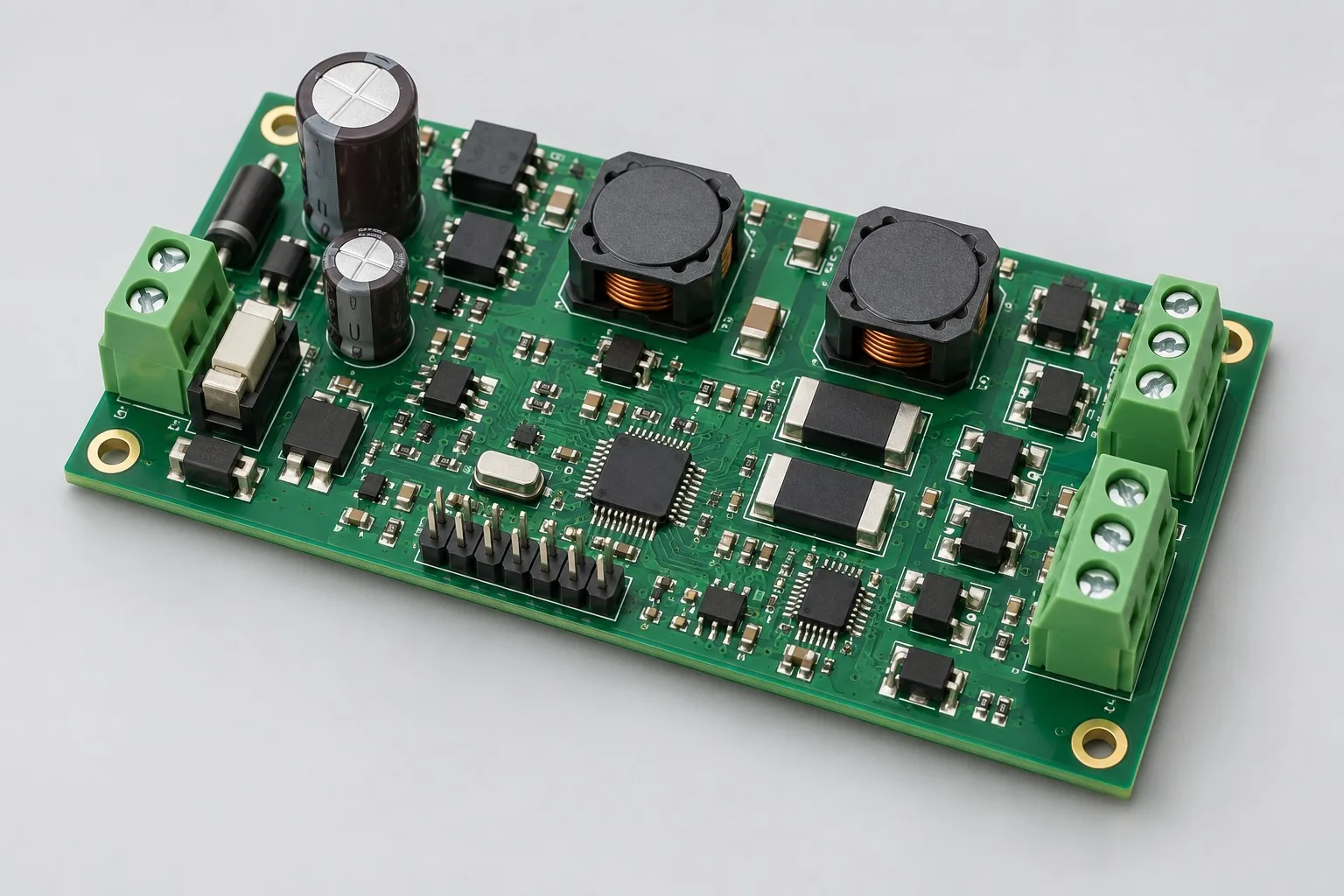
Design LED circuits around string arrangement, current regulation and fault behavior. Define dimming, thermal and prototype validation requirements.
View Design Requirements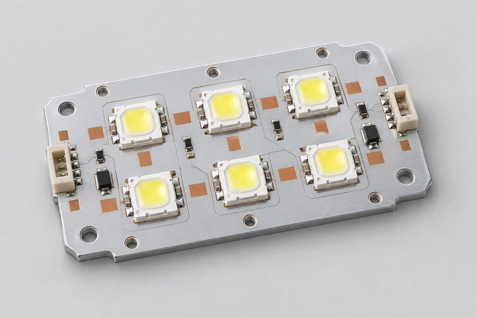
Plan metal-core LED PCB layouts with the light-source arrangement and thermal path. Coordinate dielectric insulation, mounting and external drivers.
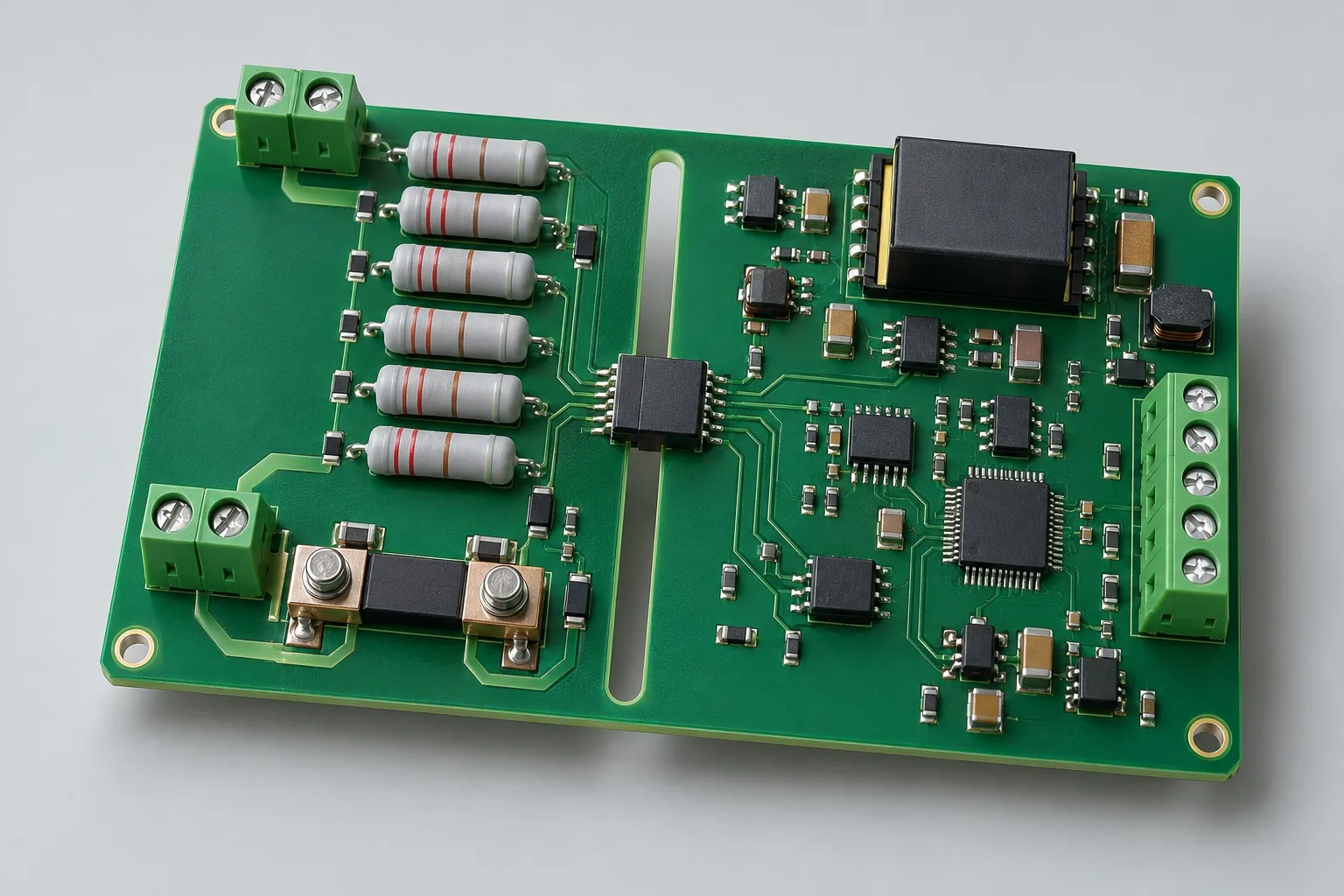
Plan high-voltage PCB design around isolation, sensing, power and fault behavior. Agree applicable safety requirements and prototype verification.
View Design Requirements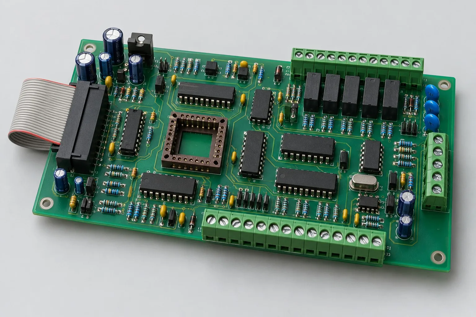
Plan authorized PCB reverse engineering from existing boards and available files. Define ownership, recovered deliverables and verification limits.
View Design Requirements
Tell us the product use and which files are available. We can define the next engineering step even when the data package is not complete.