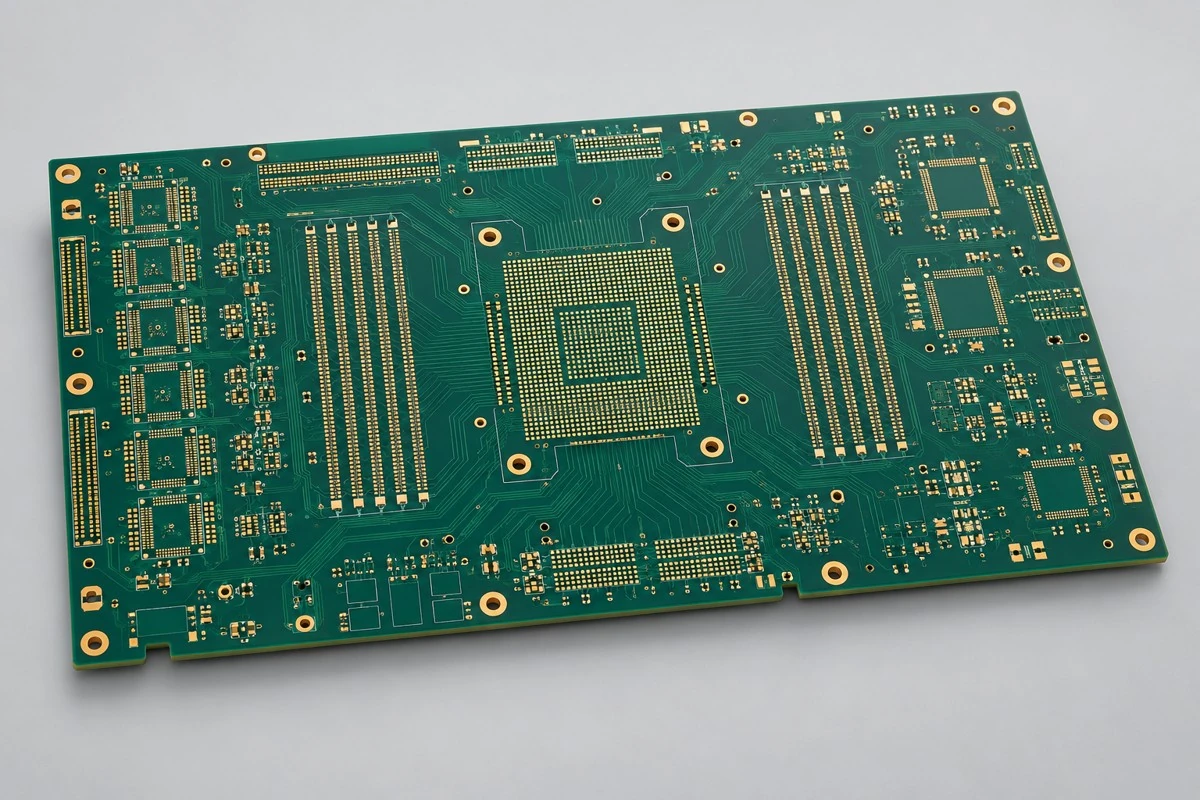
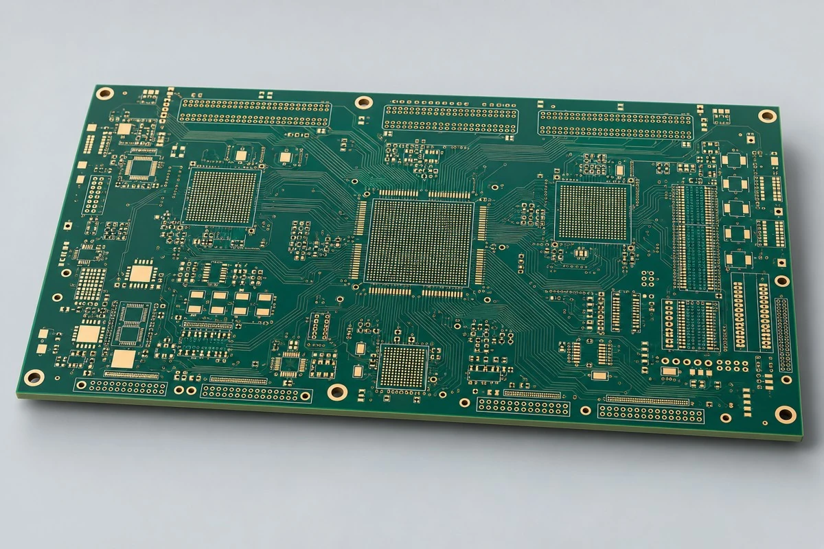
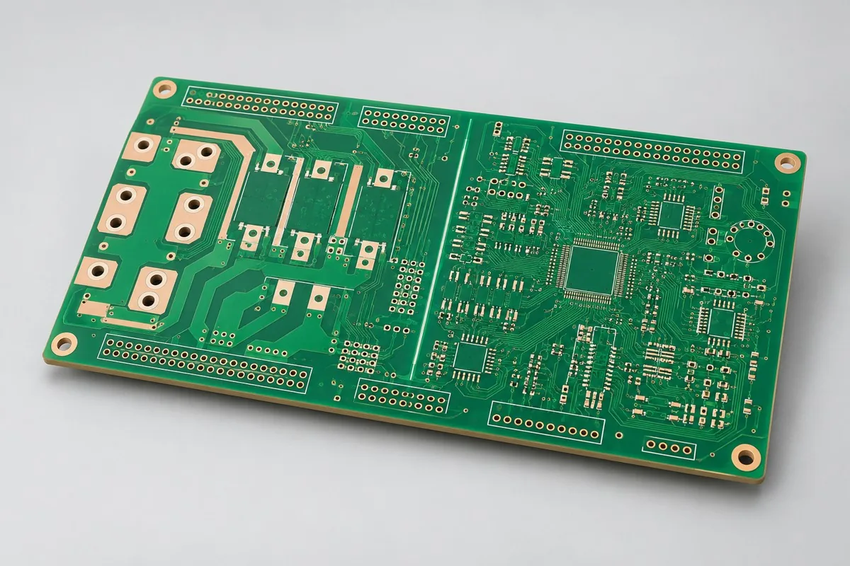
Multilayer PCB fabrication from a complete stack definition
KFPCBA provides PCB fabrication with assembly and design coordination. For a multilayer board, the starting point is a controlled layer stack, drill map and fabrication package, rather than a layer-count label alone.
Bring the circuit's power, transmission and mechanical requirements into the manufacturing review. Discuss the actual material, copper, dielectric and interconnect choices together before comparing quotations.
Specify the construction by layer and region
| Definition | What it should contain | Question to close |
|---|
| Layer stack | Named copper layers, dielectric materials and thicknesses, copper definition and final thickness | Does the released drawing distinguish design intent from an unapproved standard stack? |
| Interconnects | Plated and non-plated holes, each via span, fill/cap requirements and proposed sequence | Do drill files and cross-sections describe the same layer connections? |
| Critical transmission paths | Net or geometry identifiers, impedance requirement, reference planes and coupon relationship | What method and records establish the agreed characteristics? |
| Mechanical and assembly interface | Outline, slots, connectors, pads, component and panel requirements | Will the fabricated structure fit the intended assembly and inspection route? |
Select materials without losing the controlled revision
A material family or Tg designation does not completely specify a multilayer construction. Identify the approved grade, stack relationship and the properties relevant to the actual circuits. A proposed substitution should show what changes and which checks are required before approval.
Use material planning, the stackup checklist and material substitution guidance together. For dense package escape, a separately drawn HDI structure may be appropriate; do not infer it from the layer count.
Compare a prototype and repeat order on the same basis
Separate file preparation, tooling, material and fabrication, electrical testing, specified coupons or sections, packing and freight. Align accepted board quantities, panel delivery, material grade and construction before comparing totals.
The PCB quotation comparison helps identify exclusions. A prototype review may lead to a changed stack or via span; freeze those changes before using the prototype as the basis of a production quotation.
Agree what evidence accompanies the boards
Inspection records should identify the fabricated revision, lot or units, checked characteristics and acceptance basis. Connectivity, geometry and controlled transmission require different evidence. Link any requested coupons and sections to the construction they represent.
For subsequent assembly, keep the BOM and placement package consistent with the approved PCB revision. If the design needs further layer or constraint work, use multilayer PCB design before fabrication release.
Discuss a multilayer PCB build or send the available stackup and files through the engineering RFQ.