Company Address
201, Factory 6, Longhui Industrial Park, Fuqiao 3rd District, Xinhe Community, Fuhai Street, Baoan District, Shenzhen, Guangdong, China

Multilayer PCB Design

Plan multilayer PCB design for acquisition, industrial Ethernet and current-loop circuits. Define reference planes, isolation, clocks and calibration needs.

Multilayer PCB design around references, interfaces and manufacture

Discuss multilayer PCB design with KFPCBA when your circuit needs a controlled arrangement of routing, power and reference layers. Start from the electrical and mechanical task, then decide which structure supports it.

Adding layers can provide routing and reference options, but it does not automatically solve return-path, power-noise or connector problems. Agree the circuit responsibilities, stackup review and prototype acceptance method before detailed layout.

Define the layer and constraint strategy together

Design inputReview decisionOutput to retain
Interfaces and component escapeGrouping, timing/geometry constraints and route transitionsNet constraints and the device documentation that supports them.
Power and reference systemSupply/current paths, reference continuity, isolation domains and decouplingPower/reference map and explicitly reviewed crossings or exceptions.
Fabrication structureMaterial system, copper, dielectrics, hole spans and proposed constructionControlled stackup and fabricator review questions.
Mechanics and assemblyOutline, mounting, connectors, heights, accessible test points and panel needsA consistent electrical/mechanical layout and assembly handoff.

Keep prototype checks tied to the design purpose

For an acquisition board, define reference, analog input, timing and data-capture conditions. For a communications or control board, identify the actual interfaces, external connections and operating states. Decide which observations will establish acceptance before building the samples.

The PCB design brief helps turn these tasks into inputs. Where timing or fast edges dominate, use the high-speed design review rather than relying on a general layer-count rule.

Deliver a design package that can be maintained and built

  • Agree source files, tool and library versions, constraints and design-rule exceptions.
  • Export fabrication and assembly files from the same approved revision.
  • Check layer mapping, drill spans, board outline, material notes and critical-net requirements independently.
  • Retain prototype methods, actual observations, accepted deviations and unresolved issues.

The design-to-manufacturing checklist connects this work to multilayer fabrication and PCB assembly.

Compare layout work with complete development scope

Routing supplied schematics differs from architecture, circuit selection and prototype debugging. Agree firmware, modeling, specialist measurements and source-file rights separately. Use the development cost guide to compare deliverables, not only totals.

For an initial design enquiry, send the functions, existing circuit information, mechanical envelope and target delivery stage. Missing inputs can become a defined review task instead of an assumed design requirement.

Need a Design Direction for Your Project?

Send the product functions, interfaces, mechanical constraints, available files, and required development stage. Compare design capability scope and development support before defining deliverables.

Send Requirements

Design Directions and Functional Configurations

Compare reference designs by function, interfaces, and mechanical constraints, including design tradeoffs and prototype-acceptance methods.

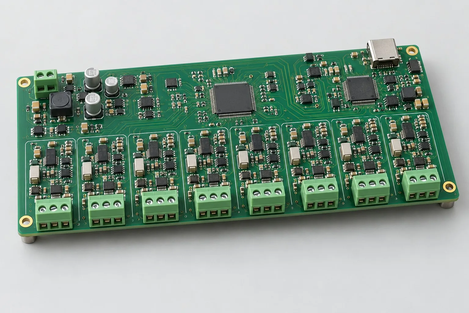
Illustrative board concept for Eight-channel synchronous acquisition board design
Engineering Reference Design · Prototype Validation Required

Eight-channel synchronous acquisition board design

Eight-channel simultaneous acquisition board design: request separate quotations for eight front ends/error budgets, common clocks, SPI buffering/upload, and per-channel calibration. 8kSPS per channel is a reference target; align input ranges, storage formats, and upload endpoints when comparing quotations. PCB-only work cannot be compared directly with development including host calibration software.

Acquisition Channel
8 differential input reference requirements
Power Supply Objective
24V DC input; independent low-noise 3.3V analog domain
Stackup Candidate
6 layers; partition analog/digital by current loops
Communication Interface
SPI to MCU; RS485 or Ethernet upload
Component Candidate
ADS131M08-class 8-channel simultaneous ADC + MCU
View Architecture, Deliverables, and Acceptance
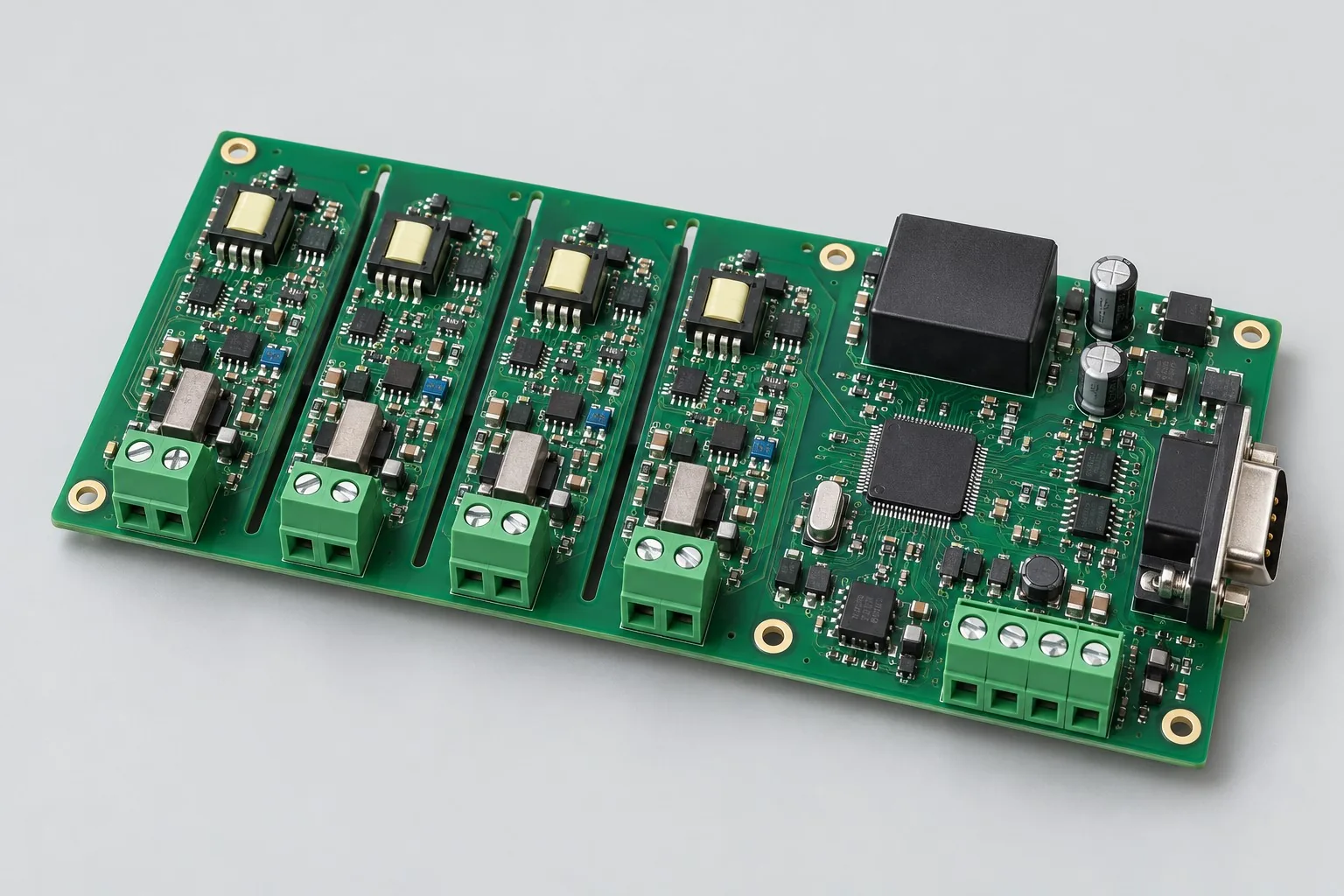
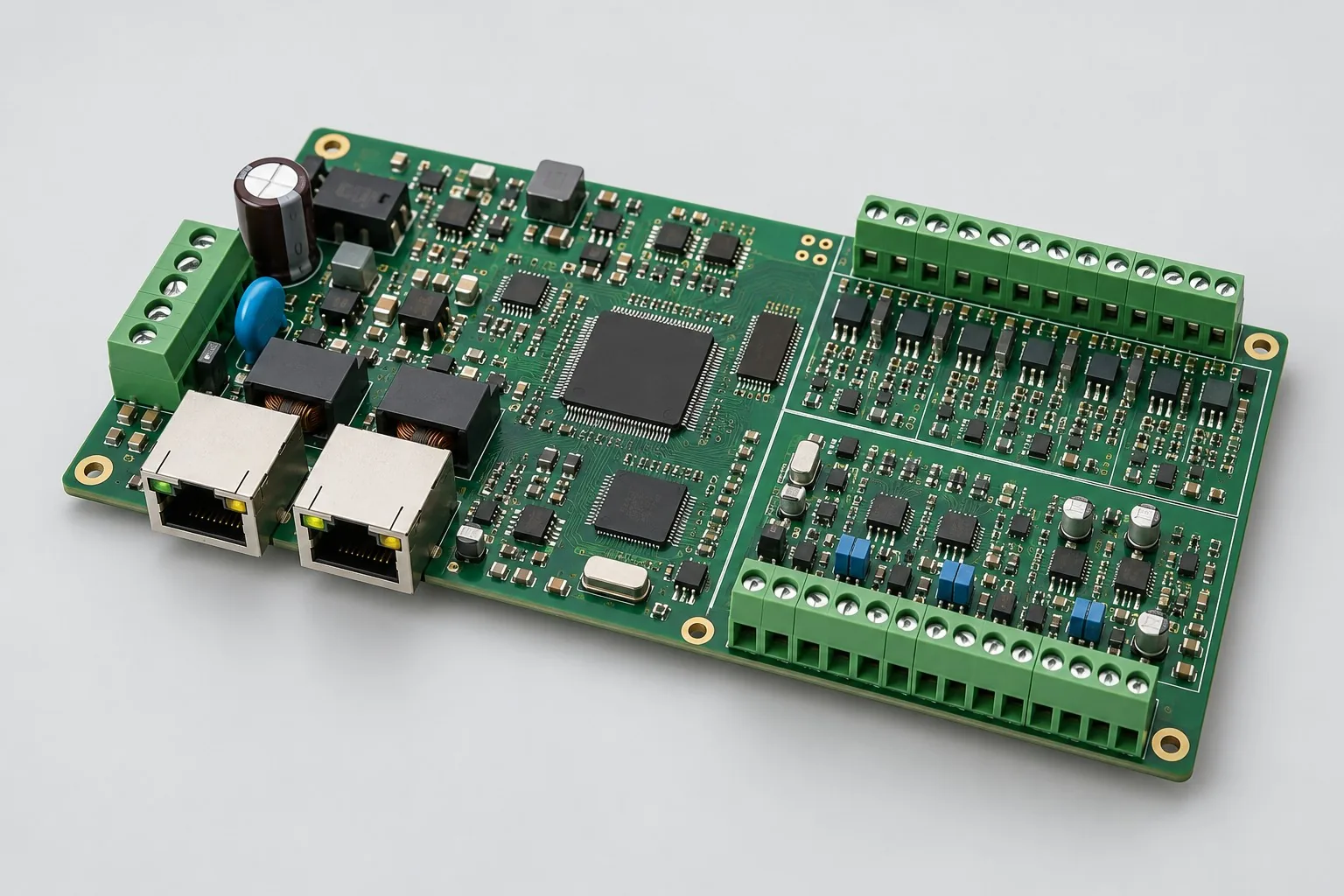
Illustrative board concept for Industrial Ethernet control board design
Engineering Reference Design · Industrial-Control Extension

Industrial Ethernet control board design

Industrial Ethernet control board design: list endpoints and tasks for reference 1-port 10/100M, 2-port RS485, optional CAN, and 8 inputs/4 outputs. Hardware includes input protection, PHY, and field I/O; software includes protocols, logs, and rollback. Quote network-saturated/concurrent-load prototypes separately rather than estimating all industrial development from one Ethernet port.

Finished Product Function
Equipment monitoring, data aggregation, control logic
Operating Input
24V DC nominal, input surge/reverse-polarity protection
Stackup Candidate
6 layers, continuous ground and separate power-distribution layers
Network Interface
1-port 10/100M Ethernet requirement target
Field Interfaces
2 RS485 ports + 1 optional CAN port
View Architecture, Deliverables, and Acceptance
Illustrative board concept for 4–20 mA acquisition board design
Engineering Design Reference

4–20 mA acquisition board design

Define a four-channel 4–20 mA acquisition board around transmitter wiring, loop headroom, input errors, and field ground potentials. Compare shared-ground sensing with per-channel isolation, and specify calibration, diagnostics, and communication.

Reference Function
Four-channel 4–20 mA transmitter acquisition
Power Target
24V field input; budget sensor supply separately
Stackup Candidate
Four layers; field-side and controller-side isolation barrier defined
Communication Interface
Isolated RS485, optional Modbus RTU
Channel Structure
Four shared-ground low-side shunts + digital isolation; assess channel isolation separately
View Architecture, Deliverables, and Acceptance
PCB / PCBA · PROJECT ENQUIRY

Does Your Project Need PCB Fabrication, Assembly, or Box Build?

Tell us the product use and which files are available. We can define the next engineering step even when the data package is not complete.

Call UsWhatsAppRequest a Quote